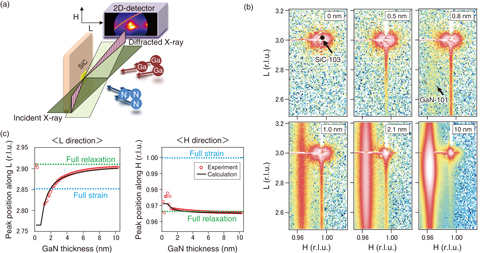
Fig.5-47 In-situ synchrotron X-ray diffraction during the growth of gallium nitride (GaN) films
Gallium nitride (GaN) is widely used for LEDs and high-frequency power devices and has the potential to drastically reduce power consumption beyond what has been achieved by conventional materials such as silicon (Si) or gallium arsenide (GaAs). Thus, a further spread of GaN-based devices is expected to help realize a future low-energy society. Despite these technological advances, many challenges affecting the crystal growth of GaN still remain. For example, surface structures, lattice deformation, and detailed defect structures in GaN films have not been fully clarified. Understanding such fundamental knowledge in terms of crystal growth is imperative for dramatically improving device performance. In this study, the lattice deformation of the GaN film is observed in real-time and a new deformation model that defies conventional theory is proposed.
Experiments were performed at the SPring-8 synchrotron-radiation facility (Beamline 11XU) using a plasma-assisted molecular-beam-epitaxy system that is directly coupled to the X-ray diffractometer (XRD). As shown in Fig.5-47(a), in situ X-ray diffraction was measured while a GaN film was grown on a silicon carbide (SiC) substrate. Fig.5-47(b) shows typical obtained experimental data. The diffraction peak of GaN was confirmed to emerge as the thickness of the GaN film reached 0.8 nm, corresponding to approximately two atomic layers. This means that our real-time measurement is quite effective at evaluating lattice deformation quantitatively at the atomic-layer scale. Fig.5-47(c) shows film-thickness dependences of the diffraction-peak positions along the out-of-plane (L) and in-plane (H) directions. These positions are related to the reciprocal of the lattice spacing of GaN in each direction. In the conventional strain relaxation of crystals, the lattice spacing of the L-direction is varied in conjunction with that of the H-direction. That is, when a film with a larger lattice constant than the substrate is relaxed, the decrement in the lattice spacing along the L-direction is almost identical to the increment of that along H-direction; this is known as conventional elastic theory. However, Fig.5-47(c) shows that the variation in the H-direction is small compared with that in the L-direction. In order to understand this anomalous phenomenon, a new lattice-deformation model reflecting lattice expansion due to the incorporation of point defects (Ga anti-site defects) was considered and a good fitting result for experimental data was obtained, as shown by the calculation result of Fig.5-47(c). This suggests that depending on the growth condition, many more point defects than are expected in the general sense can be incorporated into the GaN film.
We have proposed a new lattice-deformation model of the GaN film based upon the results of real-time observation. Since this model is important for controlling the point-defect density in GaN, it is expected to optimize the growth condition for GaN films with high quality and low defect density in the future.
<Previous: 5-18 | Next: 6 HTGR Hydrogen and Heat Application Research>