 |
||
|
 |
||
|
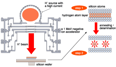
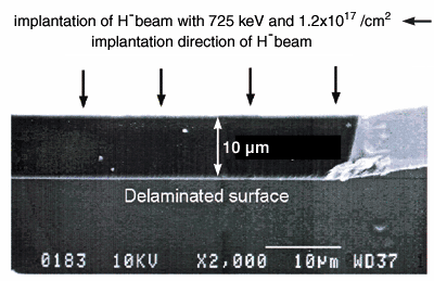
| Developed was a new technology of providing the massive and easy production of thin silicon layers by using a high-energy H- beam technology developed for nuclear fusion. The technology is expected to be used for ultra LSIs of the next generation and for future solar cells. One of the commercial methods of producing thin silicon layers is the "Delamination Method by Hydrogen Implantation," that is, the implantation of H+ ions into a single-crystal silicon at a certain depth and then the annealing of the silicon at 600°C . The above process results in the change of implanted ions to hydrogen gas, which leads to the delamination of the thin silicon layers. The disadvantage of this method is the inclusion of an amount of hydrogen molecular-ions and impurities of metal-ions and, as a result, the necessity to eliminate them from an H+ beam by use of a mass separator. The additional process has resulted in high costs and low production speed. On the other hand, the newly developed H- beam does not include hydrogen-molecular and metal ions. The technology is capable of producing a 1 MeV H- beam with a beam current of several tens of amperes and a dose area as large as a square-meter. This technology is far superior to the commercial one of producing an H+ beam of up to 200 keV with a beam current of milli-amperes and a small spot dose-area. Figure 2-19 shows the basic process of the delamination of a thin silicon layer by use of H-beam implantation. The results obtained show the feasibility of producing thin silicon layers with a production duration 100-1,000 times shorter than that of the commercial method and the production of silicon layers of 10 µm thick, though the commercial method can produce the layers of up to 2 µm thick at most. It is hoped in a near future that the results obtained contribute to the commercialization of the newly developed method of producing thin single-crystal silicon layers at low cost and the industrialization of the manufacture of solar cells with a higher energy efficiency. |
| Reference M. Hanada et al., Delamination of a Thin Silicon Layer by a High Energy H- beam, Jpn. J. Appl. Phys., (2000) in press. |
| Select a topic in left column |
|
Persistent Quest-Research Activities 2000 Copyright(c)Japan Atomic Energy Research Institute |