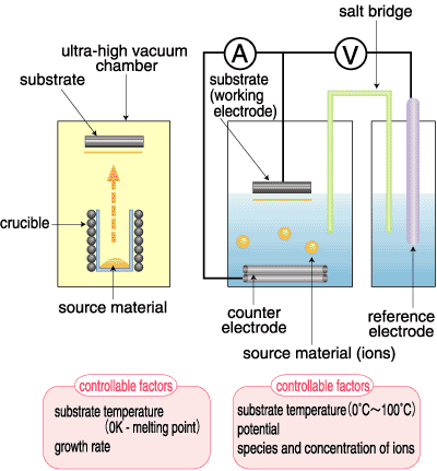
Atomic-scale control of thin-film growth is of great importance to modern and future industry. Up to now, such thin films were fabricated under ultra-high vacuum conditions to avoid adulteration. Recently, however, ultra-pure water, which is free of impurities, has been found to serve as a media equivalent to this vacuum. This finding has provoked interest in electroplating performed in ultra-pure water based solutions. As shown in Fig. 4-13, the factors affecting the growth mode of thin films are different between vacuum and solution. Hence, the electro-chemical method may allow the fabrication of films that are not possible in a vacuum. In spite of a long history of electroplating, its control in an atomic scale is still a current issue.
To establish this new technology, detailed information is required on the growth process of thin films under electrochemical conditions. Unfortunately, however, samples in solution cannot be probed by an electron beam, which is widely employed in the analysis of thin films in a vacuum. Because of the excellent penetrating feature of X-rays, however, surface X-ray diffraction plays a very important role in the study of electrochemical systems.
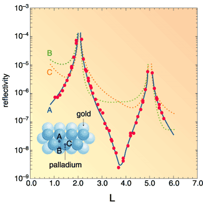
Figure 4-14 shows an example of a palladium thin film, an important catalyst. Surface X-ray diffraction techniques combined with synchrotron radiation have revealed that a palladium film with a thickness of one atomic layer can be grown on the Au(111) surface by an electrochemical method. The palladium film succeeds the crystal structure of the Au(111) substrate and has an in-plane lattice parameter identical to that of the substrate. Such a palladium film cannot be obtained in a vacuum, where islanding and alloying inevitably take place. |