Artificial satellites orbiting the earth are becoming increasingly important in our lives and now find uses in broadband communications, planetary weather pattern measurements and the investigation of environmental issues such as the depletion of the ozone layer. Electronic components designed for space must pass a stringent set of tests based on their size, weight and reliability when subjected to the harsh radiation environment of space. Space radiation, such as cosmic rays accelerated by the suns geomagnetic fields, can severely degrade the performance of a device, possibly rendering the satellite useless. Single ion strikes in a device can cause single event phenomena ranging from Single Event Upset (SEU), or soft errors, to catastrophic burn-out which physically destroys a device. An SEU occurs when the amount of charge generated by a single ion passing through a device exceeds the critical amount required to maintain the state of the circuit. In recent years the Silicon-On-Insulator (SOI) structure has become increasingly important for reducing the susceptibility of a device to SEU, by blocking a portion of the generated charge from reaching device nodes. However, charge transportation resulting from heavy ion strikes is complex, and a better understanding of the physics can be obtained by directly measuring the ultra-fast transient current produced by the ion. The system developed
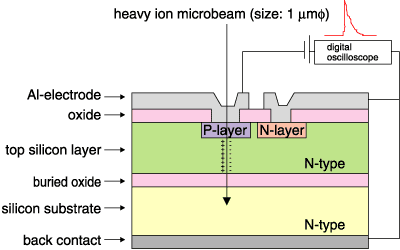
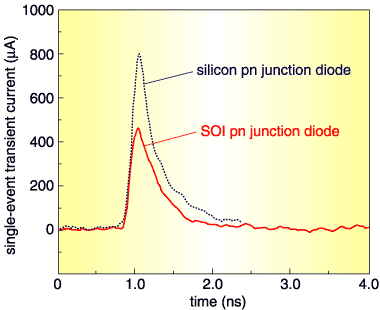
at the Takasaki Establishment uses an ultra-fast sampling system (picosecond timing resolution) for measuring transient currents in conjunction with a high-energy heavy ion microbeam attached to a 3 MeV tandem accelerator. Using this system we have measured the transient currents resulting from 15 MeV O, C and Si ion strikes in SOI pn diode test structures as depicted in Fig. 5-1. Shown in Fig. 5-2, are two examples of transient currents collected from an SOI and bulk Si diode respectively. As shown, the peak transient current has been reduced by the use of a buried oxide layer. By carefully comparing the amount of charge deposited within the device to that measured by integrating the transient current, it has been concluded that SOI is indeed an effective means of increasing the radiation tolerance of a device. Indeed the exact positioning of the oxide can be used to control the amount of charge collected from an ion strike. This knowledge, together with further investigation, will better aid future design of electronic devices intended for space applications. |