Semiconductors are widely used for electronic and optoelectronic devices. Many semiconductors, such as GaAs, InP, CdTe, etc., contain the elements As, In, Se, etc., which only occur in limited quantities naturally. Furthermore, some of these elements (As, Cd, etc.) are harmful to human health. These elements could quite possibly have an adverse influence on human life as well as on the environment, if devices containing them are disposed of as waste. From the viewpoint of environmental and ecological safety, these elements should be avoided for the purposes of device fabrication. We have investigated the fabrication of silicide semiconductors as "ecologically friendly" materials.
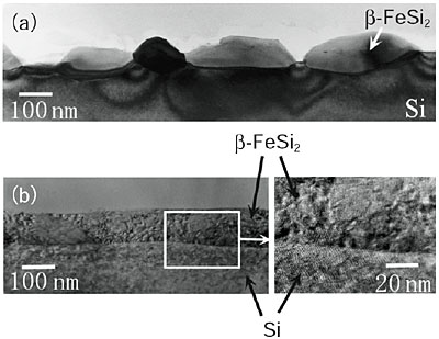
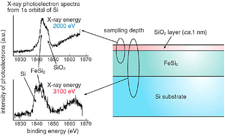
Among these compounds, beta-FeSi2 is a promising candidate as a photo sensor or a thermoelectric device. beta-FeSi2 is expected to have excellent optical and electrical properties according to spectroscopic measurements and band structure calculations. It is also expected that this compound will have strong radiation resistance. However, thin, uniform films are hard to obtain, since iron silicide aggregates easily during the conventional formation processes. We have succeeded in fabricating highly oriented, uniform beta-FeSi2 films of 100 nm thickness using the ion beam sputter deposition method under ultra high vacuum conditions by controlling the substrate surface treatment (Fig. 8-5). Moreover, no significant changes from oxidation can be observed on the film surfaces formed by this way after several months following fabrication in air. The depth profile of the film obtained was observed non-destructively using synchrotron radiation X-ray photoelectron spectroscopy. The results show that a very thin SiO2 layer (1 nm) covers the beta-FeSi2 film (Fig. 8-6). Strong oxidation resistance for beta-FeSi2 is therefore achieved.
Such highly-oriented, uniform films offer improved material properties in applications such as semiconductor devices. These techniques will be extended to device fabrication studies in the near future.
|