Most semiconductor devices used in modern personal computers are of elemental silicon (Si) composition. Due to recent rapid progress in nanotechnology, it has become important to fabricate ultra-thin layers and ultra-small particles (clusters) made of Si atoms. Especially, the quantum-dot, whose diameter is less than 10 nm, has excellent properties such as highly efficient visible-light emission and highly brilliant electron emission. Thus, it is of great importance to elucidate the geometric and electronic structures of nano-scale Si materials.
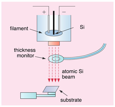
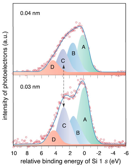
In the present study, ultra-thin films of elemental Si were deposited on solid surfaces using precisely controlled atomic Si beams (Fig. 5-18). The surface electronic structures were analyzed by X-ray photoelectron spectroscopy and X-ray absorption spectroscopy using soft X-rays from the synchrotron radiation facility. Fig. 5-19 shows the X-ray photoelectron spectra around Si 1 s orbitals of deposited Si atoms for thin (0.04 nm) and ultra-thin (0.03 nm) films. The main peak A corresponds to bulk Si. New photoelectron peaks were observed on the higher energy side than in the bulk Si. It was found that the peak C grew with a decrease in the thickness of the film. In comparison with the theoretical calculation, we conclude that peak C originates from clusters consisting of ten Si atoms. It is also elucidated that the synthesized clusters resist oxidation better than bulk Si.
For the first time, the electronic structures of nano-scale Si were understood to be quite different from those of bulk Si solids. The present results will surely contribute to the understanding of the unique properties of nano-scale Si, such as the quantum-dot. |

