Silicon (Si) semiconductors are widely employed in many electronic
devices such as computer memories. For such uses, Si is generally
prepared by a series of processes: ion implantation, etching,
thermal oxidation, and washing. Unfortunately, the ion implantation
is inevitably accompanied by defect formation and amorphization
of the crystal, and the washing often contaminates the crystal
with hydrogen atoms. The resulting defects and atoms play decisive
roles in determining the properties of recent semiconductor devices,
for which sub-micrometer processing is required.
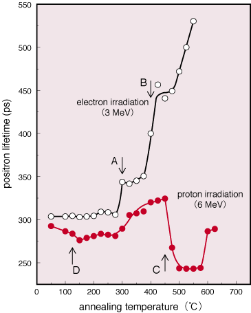
Using positron lifetime measurements, we are studying the behavior
of defects and hydrogen atoms in Si which have been introduced
artificially by electron- or proton-irradiation. A positron, having
the same properties as an electron except that it has a positive
charge, will be trapped in a defect (i.e. vacancy in the crystal)
to combine with an electron and eventually disappear. Measurements
of positron lifetimes can therefore give us information on the
defect structures at the atomic level which no other method can
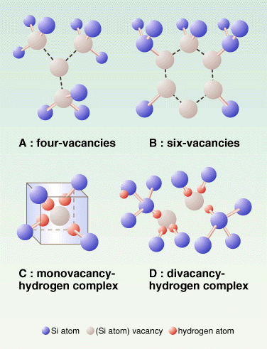
provide. Using this method, we found that, in N-type semiconductors,
an increase in the temperature makes the defects (e.g. vacancy-phosphor
atom pairs) migrate and recombine to produce stable vacancy-type
defects, e.g., four- or six-vacancies. The method was also used
to elucidate the formation process of the vacancy-hydrogen atom
complexes. |