4.3 High Temperature and Radiation-Resistant Semiconductor Devices for the Next Stage
- Fabrication of a Silicon Carbide Transistor-

Fig. 4-5 Defect density in a SiC crystal as a function of implantation temperature
Defects produced by 200 keV N2+ ion (n-type impurity) and Al+ ion (p-type impurity) implantation into a SiC single crystal (film thickness: 30 micrometers) were measured with the electron spin resonance technique. By hot implantation at 800 degrees, the concentration of defects greatly decreases by a factor of a hundred compared to room-temperature implantation. By contrast, Al+ ion implantation at temperatures higher than 800 degrees increases the defect density. Hot implantation with less defect production and post-heat annealing permit the fabrication of electrically active p-type and n-type SiC semiconductors.

(b) SiC MOS transistor under magnification
Fig. 4-6 SiC MOS transistor fabricated by hot implantation
Electric current (on, off) from source electrode to drain electrode is controlled by the voltage at the gate electrode (Fig. (a)). Many such transistor structures are integrated on a crystalline substrate to obtain an integrated circuit (IC) (Fig.(b)).


For materials to be used as electronic devices in strong radiation fields such as in spacecraft or in nuclear power plants, silicon must be replaced by other suitable materials because it is easily damaged by radiation. We have been studying silicon carbide (SiC) as a promising material for high power, high temperature and radiation-resistant devices.
To make SiC transistors, introduction of impurities into SiC crystals as in ion implantation is required to get p-type and n-type conducting layers. Conventional ion implantation does not produce electrically activated impurities, however. We therefore focussed our attention 
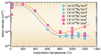
on hot implantation, and implanted nitrogen ions of donor into a p-type SiC single crystal substrate heated to 1,000 degrees. It turned out that this reduces implantation-induced defects significantly (Fig. 4-5) and simultaneously converts n-type SiC into p-type SiC after the electrical activation of the implanted nitrogen. 
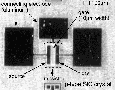
As for a MOS (metal/oxide/semiconductor) structure, we fabricated a radiation-resistant MOS structure, two orders of magnitude stronger than silicon, by oxidizing the surface of the SiC substrate at 1,100 degrees under a mixed gas atmosphere (H2O+O2) with H2O being produced by burning hydrogen. By using the hot-implantation and the MOS fabrication techniques, we can obtain radiation-resistant SiC MOS transistors (Fig. 4-6).


Reference
H. Itoh et al., Characterization of Residual Defects in Cubic Silicon Carbide Subjected to Hot-Implantation and Subsequent Annealing, J. Appl. Phys., 82 (11), 5339 (1997).

Select a topic in left column


Persistent Quest-Research Activities 1998
Copyright(c)Japan Atomic Energy Research Institute