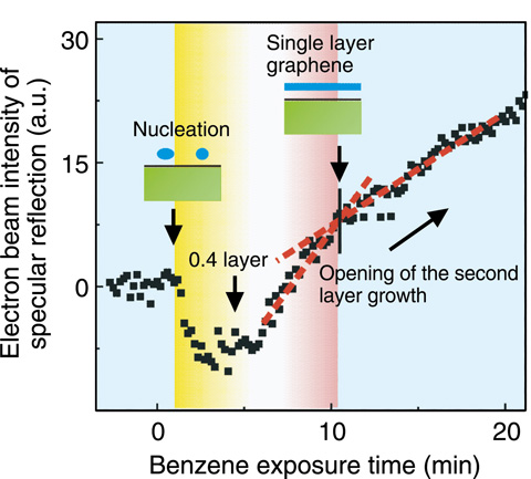
Fig.7-6 Evolution of the electron beam intensity during the growth of graphene
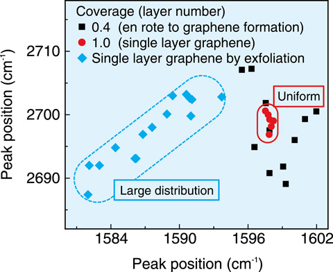
Fig.7-7 Uniformity of the atomic and electronic structure of graphene
Since the discovery of a convenient method for the fabrication of graphene via micromechanical exfoliation from bulk graphite (2010 Nobel Prize in physics), graphene has attracted world-wide attention as an innovative nanoelectronic material. In the field of spintronics, graphene is expected to be an ideal spin-transport material owing to its extremely long spin diffusion length and high carrier mobility. However, the non-uniformity in both the number of carbon layers and the electronic states of exfoliated graphene is making it difficult to control the spin transport properties. Therefore, a new fabrication method that enables the tailoring of graphene is indispensable for the development of spintronic applications.
In this study, we focused on a chemical growth method for graphene. A graphene film was synthesized by exposing a metal (nickel) to precursor (benzene) vapors. The growth process for graphene was monitored via in situ analysis of the electron beam intensity of the specular reflection (Fig.7-6), and it was successfully demonstrated that the nucleation and step flow of the graphene growth process can be simultaneously monitored by the change in the specular beam intensity. This approach makes it possible to obtain graphene with a uniform layer number through precise control of the growth conditions. In addition, it was found that a remarkably high uniformity of the electronic states of our graphene compared to that of the exfoliated graphene can be achieved by adjusting the exposure conditions used to complete the growth of a single carbon layer, as shown in Fig.7-7.
Use of this tailored synthetic method should enable efficient control of the spin transport properties of graphene and lead to the development of graphene-based spintronic and nanoelectronic devices.
<Previous: 7-2 | Next: 8 Nuclear Science and Engineering Research >