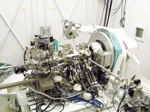
Fig.4-24 X-ray diffractometer integrated with a molecular beam epitaxy chamber
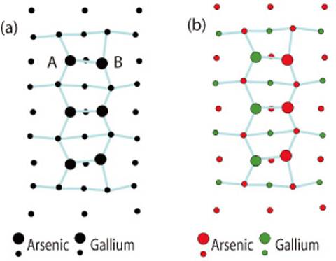
Fig.4-25 Surface structure of gallium arsenide under growth conditions
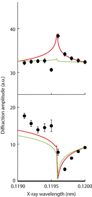
Fig.4-26 Diffraction amplitude as a function of X-ray wavelength
Gallium arsenide is a semiconductor showing excellent performance in optoelectronic and high-frequency devices. It is playing a critical role in today's highly-networked society as widely used in cell phones and optical communication lasers. For these applications, atomically-controlled device structures are grown using state-of-the-art techniques called molecular-beam epitaxy (MBE) and metalorganic chemical vapor deposition (MOCVD). These techniques need detailed knowledge about surface structures during growth.
We have developed an X-ray diffractometer integrated with an MBE chamber (Fig.4-24) at "SPring-8" for surface studies during crystal growth. The intense X-rays of "SPring-8" have speeded up the measurements of surface X-ray diffraction, which is weaker than the diffraction from bulk crystals by several orders of magnitude. Moreover, a wide spectrum of SPring-8 X-rays has enabled the determination of the species of surface atoms as well as their coordinates.
Fig.4-25(a) shows the top view of the gallium arsenide surface investigated in the present work. Conventional surface analysis techniques have difficulty in differentiating between gallium and arsenic because the numbers of electrons possessed by gallium and arsenic are fairly close, being 31 and 33, respectively. In fact, in Fig.4-25(a), each atom is indicated by a circle whose radius is proportional to the number of the electrons it has, but the difference is subtle. In the present study, We investigated the variation of X-ray diffraction intensity as a function of X-ray wavelength. As shown in Fig.4-26, the experimental results (filled circles) agree better with the model in which the topmost layer consists of both gallium and arsenic (red lines) than the counterpart in which only arsenic is present on the surface (green lines). In the sense of using multiple wavelengths, this method is equivalent to taking a color picture like Fig.4-25(b), in which gallium and arsenic atoms can be distinguished easily.
The X-ray technique is suitable for industry-oriented MOCVD growth as well because X-rays can propagate even in high ambient pressures which are typical for MOCVD. This method is expected to accelerate the development of novel devices through precise control of semiconductor processes.