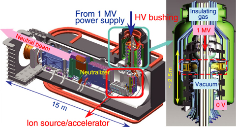
Fig.3-9 ITER NBI system and high voltage bushing
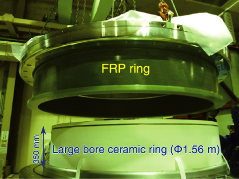
Fig.3-10 Full-size mockup of high voltage bushing
Neutral beam injection (NBI) is one of the key technologies for plasma heating and current drive in ITER. In the ITER NBI, a 1 million volt (MV) electrostatic accelerator is equipped to produce deuterium negative ion beams. A conventional insulation method to sustain high voltage in an accelerator is gas insulation with SF6 gas. However, the accelerator in the ITER NBI is exposed to a radiation environment and electric current is induced in the insulating gas in such an environment, which results in power dissipation, and thus the accelerator must be installed in a vacuum. A high voltage (HV) bushing is then required to be mounted between the transmission line from the 1 MV power supply in the SF6 gas and the accelerator in the vacuum. The HV bushing, which acts as a bulkhead and a feedthrough, is composed of a five-stage insulator to sustain 1 MV insulation (Fig.3-9). Since many conductors must be located inside the ceramic ring sustaining 1 MV insulation, the dimensions of the ceramic ring must be 1.56 m in diameter, 29 cm in height, and 5 cm in thickness. However, in conventional manufacturing methods the diameter has been limited to less than 1 m, and hence to establish a manufacturing method for the large ceramic ring has been a long-standing issue, for over ten years. To make the HV bushing a reality, JAEA and Kyocera Cooperation succeeded in manufacturing the world’s largest ceramic ring (1.56 m in diameter) with a newly-developed forming method. A joining technique by brazing of the large ceramic ring with Kovar (a nickel alloy) was also developed in collaboration between JAEA and Hitachi Haramachi Electronics Co., Ltd.
JAEA manufactured a full-size mockup with the brazed ceramic, which simulated one stage of the HV bushing, as shown in Fig.3-10. To suppress breakdown triggered at the joint of the ceramic and metal, stress rings developed in R&D activity for the ITER accelerator in JAEA were installed in the mockup.
In the high voltage test of the mockup, 240 kV were sustained stably for over 1 hour. This is 20% higher than the rated voltage for each ceramic ring (200 kV), and thus the voltage holding capability required in the ITER NBI was verified for the first time. The present result supports development of the ITER NBI. Application of the vacuum insulation technique is expected to promote development of a “SF6 gas free” high voltage component, which will be useful in the power industry.