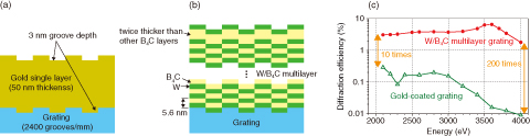
Fig.5-28 Schematics of (a) a gold-coated grating and (b) an aperiodic W/B4C multilayer grating. (c) The measured diffraction efficiencies of both gratings are plotted as functions of photon energy at a constant angle of incidence
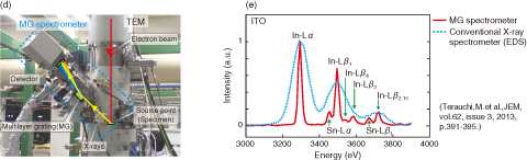
Fig.5-29 MG spectrometer installed in (d) a TEM and (e) emission spectra from ITO
Electron microscopes (EMs) are useful tools for the structural analysis of materials at nanometer scales. X-rays are generated when a material is irradiated by an electron beam. If the X-ray intensity distribution is plotted as a function of the photon energy by using an X-ray spectrometer with a diffraction grating featuring many narrow grooves on its surface, we can analyze the valence electronic structure underlying the material properties. As conventional soft X-ray gratings are coated with a thin gold film, their use becomes impractical at energies around the gold absorption edges (approximately 2.2 keV). To overcome this problem, we designed an aperiodic W/B4C multilayer structure and applied it to a wideband multilayer grating covering 2.0-4.0 keV at a constant angle of incidence.
Fig.5-28 presents schematics of an Au-coated grating (AG) (a) and the designed aperiodic W/B4C multilayer grating (MG) (b). The measured diffraction efficiency curves of both gratings are plotted in panel (c). The diffraction efficiencies of the MG at 2.1 keV and 4.0 keV are 10 and 200 times higher than those of the AG, respectively. The MG also shows uniformly high efficiency over the entire energy range. This result is attributable to the reflective characteristic of the B4C layer just below the topmost W layer, whose thickness is twice that of the other layers in the structure, as shown in Fig.5-28(b).
Fig.5-29 is a photograph of the MG spectrometer installed in a transmission EM. Also shown are the emission spectra from indium-tin-oxide measured by the MG spectrometer and a conventional energy-dispersive spectrometer (EDS). The L emission spectra of Sn and In (e.g., Sn-Lα and In-Lβ1) are more clearly resolved by the high-resolution MG spectrometer than by EDS.
By combining X-ray spectroscopy with EM, we have established a unique technique for extracting morphological and electronic structure information. This technique is expected to assist the development of electronic devices and functional materials.
The present study was partly supported by the project of Collaborative Development of Innovative SEEDs from the Japan Science and Technology Agency (JST).