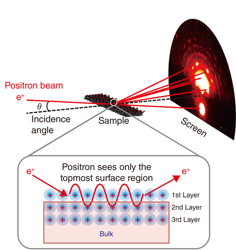
Fig.3-7 Setup of total-reflection high-energy positron diffraction (TRHEPD) experiment

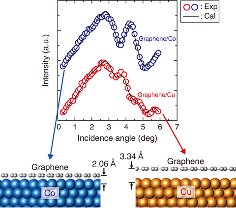
Fig.3-8 Intensity of diffracted positrons for graphene/Co and graphene/Cu and analytical results
Recently, graphene, a two-dimensional atomic sheet of carbon, has been extensively investigated with a view to potential applications in future energy-saving and high-speed devices. Graphene, the discovery of which was awarded the 2010 Nobel Prize in Physics, is well known to have many promising features, including high carrier mobility and robust mechanical properties. There have been many studies on the properties of free-standing graphene. However, the properties of graphene in contact with other substances remain largely unknown. Because graphene has a very thin, one-atomic-layer thickness, its properties may be affected by substances with which it is in contact. In order to clarify this, it is necessary to investigate the graphene itself and the interface between the graphene and its substrate. Analyzing such a thin region near the topmost surface layer is difficult. Therefore, there are strong demands for experimental methods with limited penetration depth. We have developed a total-reflection high-energy positron diffraction (TRHEPD) technique and measured the interface between the graphene and the metal substrates. Fig.3-7 shows the experimental setup of the TRHEPD technique. Since the positron, the antiparticle of the electron, has a positive charge (opposite to that of the electron), it feels the repulsive force from materials. Thus, the positron beam does not penetrate the deeper bulk region. Therefore, the TRHEPD method enables us to accurately determine atomic configurations of the topmost- and near-surface layers.
In the present study, we fabricated graphene on two different metal substrates, namely cobalt (Co) and copper (Cu), and performed the TRHEPD experiments. We found that the peak positions of the diffracted positrons for the Co and Cu substrates are significantly different (Fig.3-8). As a result of this intensity analysis, the spacing between the graphene and the Co substrate was determined as 2.06 Å. For the Cu substrate, however, the spacing was observed to be 3.34 Å, which is more than 1 Å larger that of the Co substrate. It is known that the atomic layers of graphite, which is a stack of graphene layers, are weakly bonded to each other and that the interlayer distance is 3.3 Å. Therefore, graphene is strongly bonded to the Co substrate, whereas in the Cu case, the interaction is very weak. We experimentally verified that the bonding character of the graphene changes depending upon the element of the substrate.
Recently, two-dimensional atomic sheets such as silicene (the Si version of graphene) and germanene (the Ge version), which do not exist in nature, have been successfully fabricated on various substrates. Furthermore, atomic sheets of superconductors on insulator substrates give rise to high-temperature superconductivity. In the near future, we will investigate such novel atomic sheets and the interface with the substrate using the TRHEPD method.
This work has been conducted in collaboration with the High Energy Accelerator Research Organization (KEK).