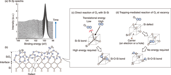
Fig.1 Reaction of O2 molecules at the SiO2/Si interface
Transistors, which form the basic structure of integrated circuits that control the operations of computers and smartphones, are formed by oxidizing Si and creating an oxide film. In recent years, as transistors have become more densely integrated, it has become necessary to fabricate oxide films as thin as 1 nm. In such thin films, the presence of only a few defects can cause increased power consumption and malfunctions. Therefore, it is essential to precisely control the oxidation reaction and fabricate oxide films without defects. However, the oxidation reactions in atomically thin films are not well understood.
In this study, the oxidation reaction on Si surface was observed in real-time by X-ray photoelectron spectroscopy using high-brilliance, high-resolution synchrotron radiation at BL23SU in SPring-8 to clarify the oxidation reaction at the nano-level.
The oxide film (SiO2) on a Si substrate grows by O2 uptake from the oxide film surface, subsequent diffusion of O2 into the interior and reaction at the SiO2/Si interface. The reaction of O2 at the SiO2/Si interface has been considered to be a direct reaction of O2 with the Si-Si bond to form a Si-O-Si bond. However, such a process requires high-energy O2 molecules. The average kinetic energy of O2 diffusing through the film is low, making oxidation by O2 gas impossible (Fig.1(c)).
We focused on defects generated at the SiO2/Si interface by the large strain induced by volume expansion caused by SiO2 formation. We predicted that the carriers (i.e., electrons and holes) associate with defects and react with O2 in a chemically active state. We demonstrated this by obtaining the time variation of the Si 2p spectra (Fig.1(a)), which reflects the amount of interfacial carriers, by real-time photoemission spectroscopy measurements using synchrotron radiation. Furthermore, from the changes in the amount of interfacial O2, we deduced that O2 molecules are adsorbed on the defects associated with the carriers. The molecular O2 then dissociates into O atoms and forms Si-O-Si bonds. Since the reaction via such molecular adsorption requires no energy, we confirmed that the reaction proceeds along the path shown in Fig.1(d). This study proposes a new reaction mechanism in which the reaction of O2 at the SiO2/Si interface proceeds via molecular adsorption at defects, and the carrier from the Si substrate is involved in the process.
The inference that O2 reacts at defects suggests that SiO2 growth is possible while annihilating defects. Therefore, this research is expected to lead to applications with power-saving, improved reliability, and further miniaturization with performance enhancement through higher-density integration of devices.
This research was conducted in collaboration with Tohoku University and National Institute of Technology, Fukui College.
(Yasutaka Tsuda)
<Previous: 5-6 | Next: 6 Computational Science and E-Systems Research>